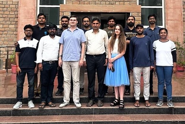
Mahesh Kumar
Associate Professor
Electrical Engineering
Lab: Micro and Nanoelectronics Lab
Address:
Department of Electrical Engineering
Indian Institute of Technology Jodhpur
NH-62, Nagaur Road, Karwar
Jodhpur 342037
India
Room: 207
Email: mkumar@iitj.ac.in
Telephone: +91 291 280 1357
Event
Sumposium on 2D Materials and Devices 27-28 September 2019 Frontiers of Science Brainstorming Meeting 4-6 November 2019 DAE Solid State Physics Sumposium 18-22 December 2019 Frontiers of Science Brainstorming Meeting 9-11 December 2018 National Conference on Semiconductor Materials and Devices 4-6 March 2016Biography
Dr. Kumar has received M.Sc degree in Physics from University of Rajasthan, M.Tech degree in Solid State Materials from IIT Delhi and Ph.D degree in Engineering from IISc Bangalore. He worked at Central Research Laboratory of Bharat Electronics Ltd. (CRL-BEL) Bangalore as Scientist from 2005 to 2013. He also worked at University of Paderborn, Germany as visiting scientist (3 months) under Bilateral Exchange Programme of INSA and at University of South Dakota, USA as Bhaskara Advanced Solar Energy Fellow (3 months) supported by Indo-U.S. Science and Technology Forum. He has received INSA Medal for Young Scientists-2014 by Indian National Science Academy,the MRSI Medal-2016 by Materials Research Society of India, DAE-Young Achiever Award-2016 by BRNS (Department of Atomic Energy), ISSS Young Scientist Award 2017 by the Institute for Smart Structures and Systems,JPhysD Emerging Leader Award 2018 from Institute of Physics (UK), YSAP mission award 2019 by Global Young Academy and PHSS Foundation Young Scientist Award 2018-19 by Prof. H. S. Srivastava Foundation. He is founding Member and served as Chair of Indian National Young Academy of Sciences, Member of National Academy of Sciences India & Global Young Academy (2017-2022) and IEEE Senior Member from 2016. He has published more than 100 research articles.
Current Research area
- Oxide metal semiconductors for Gas sensing applications
- 2D materials for Gas sensing and Photo detection applications
- III-Nitride high electron mobility transistors for heavy metal ion sensors
- Bandgap engineering and surface studies of semiconductors
- Wide Bandgap Semiconductors for Deep-UV photodetectors
- Micro and Nano device fabrications
Teaching
- Optoelectronics
- Electromagnetic Theory
- Microelectronics-II
- Sensors in Instrumentation
- Physics of Semiconductor Devices
- Introduction to Electrical Engineering
Group Members
- Amit Shringi, Ph.D
- Surajit Das, Ph.D (With Dr. Jitendra Singh, CEERI Pilani)
- Nipun Sharma, Ph.D (IDRP)
- Ashok Kumar, Ph.D
- Amit Kumar, Ph.D
- Sumit Kumar, Ph.D
- Sarvar Singh, Ph.D
Alumni
-
Ph.D
- Vijendra Bhati
- Adarsh Nigam
- Rahul Kumar
- Neeraj Goyal
- Dr. Surendra Singh Barala,Ph.D 2017,Scientist @ Defence Lab Jodhpur,DRDO
- Dr. Sapana Ranwa, Ph.D 2017, Assistannt Professor, NIT Durgapur Research Staff
- Dr. Saravanan Rajamani, National-Postdoc Fellowship (Oct 2015- Dec 2019)
- Dr. Nandlal Sharma, Research Associate (Jan 2018 to Nov 2018)
- Dr. Shushant Kumar Singh, RA (Jan 2019 to April 2019)
- Manoj Kumar Rajbhar, SRF (Sept 2018 to April 2019)
- Yogeshwaran Krishnan, SRF (May 2018 to July 2018)
- Mohit Kumar, JRF/SRF (August 2014 to June 2017)
- Shivani Agarwal, SRF (Nov 2015- July 2016)
Journal Publications
2020
101. Room-Temperature Gas Sensors under Photoactivation: From Metal Oxides to 2D MaterialsRahul Kumar, Xianghong Liu, Jun Zhang, and Mahesh Kumar Nano-Micro Letters (In Press).
100. Real time detection of Hg2+ ions using MoS2 functionalized AlGaN/GaN high electron mobility transistor for water quality monitoring
Adarsh Nigam, Neeraj Goel, Thirumaleshwara N Bhat, Md. Tawabur Rahman, Surani Bin Dolmanan, Qiquan Qiao, Sudhiranjan Tripathy and Mahesh Kumar Sensors and Actuators B: Chemical 309, 127832 (2020).
99. Single-atom catalysts boosted ultrathin film sensors
Rahul Kumar and Mahesh Kumar Rare Metals (In press).
98. Transition Metal Dichalcogenides-Based Flexible Gas Sensors
Rahul Kumar, Neeraj Goel, Mirabbos Hojamberdiev and Mahesh Kumar Sensors and Actuators A: Physical 303, 111875 (2020).
97. Highly Tunable Film Bulk Acoustic Wave Resonator Based on Pt/ZnO/Fe65Co35 Thin Films
Jitendra Sigh, Ajay Kumar and Mahesh Kumar IEEE Transactions on Ultrasonics, Ferroelectrics, and Frequency Control (In press).
96. MoS2-Based Nanomaterials for Room-Temperature Gas Sensors
Rahul Kumar, Wei Zheng, Xianghong Liu, Jun Zhang and Mahesh Kumar Advanced Materials Technologies 5, 1901062 (2020).
95. Enhanced adsorption sites in monolayer MoS2 pyramid structures for highly sensitive and fast hydrogen sensor
Abhay. V. Agrawal, R. Kumar, Guang Yang, Jiming Bao, Mahesh Kumar, and Mukesh Kumar Int. J. Hydrogen Energy 45, 9268 (2020).
94. Development of ZnO nanostructure film for pH sensing application
Manoj Kumar Rajbhar, Saravanan Rajamani, S. K. Singh, Sergey Surodin, Dmitry Nikolichev, Ruslan Kryukov, Dmitry Korolev, Alyona Nikolskaya, Alexey Belov, Alexey Nezhdanov, Alexey Mikhaylov, David Tetelbaum and Mahesh Kumar Bulletin of Materials Science (In Press).
93. Development of ZnO nanostructure film for pH sensing application
Prashant Sharma, Vijendra Singh Bhati, Mahesh Kumar, Rishi Sharma, Ravindra Mukhiya, Kamlendra Awasthi and Manoj Kumar Applied Physics A 126, 284 (2020).
92. Anisotropic Electron-Photon-Phonon Coupling in Layered MoS2
Deepu Kumar, Birender Singh, Rahul Kumar, Mahesh Kumar and Pradeep Kumar Journal of Physics: Condensed Matter (In press).
91. Highly Sensitive and Selective Detection of Acetone Based on Platinum Sensitized Porous Tungsten Oxide Nanospheres
Yongshan Xu,Chengming Lou, Lingli Zheng, Wei Zheng, Xianghong Liu, Mahesh Kumar, Jun Zhang Sensors and Actuators B: Chemical 307, 127616 (2020).
90. Enhanced sensing performance of ZnO nanostructures-based gas sensors: A review
Vijendra Singh Bhati,Mirabbos Hojamberdiev and Mahesh Kumar Energy Reports 6, 46 (2020).
2019
89. Sensitive and Selective Detection of Pb2+ ions using 2,5-Dimercapto-1,3,4-Thiadiazole Functionalized AlGaN/GaN High Electron Mobility TransistorAdarsh Nigam , Vijendra Bhati , Thirumaleshwara Bhat , Surani Dolmanan , Sudhiranjan Tripathy and Mahesh Kumar IEEE Electron Device Letters 40, 1976 (2019).
88. PAN/(PAN-b-PMMA) derived Nanoporous Carbon Nanofibers loaded on ZnO Nanostructures for Hydrogen Detection
Vijendra Singh Bhati, Akash Nathani, Adarsh Nigam, Chandra Shekhar Sharma and Mahesh Kumar Sensors and Actuators B: Chemical 299, 126980 (2019).
87. Boosting Sensing Performance of Vacancy-Containing Vertically Aligned MoS2 using rGO particles
Rahul Kumar,Neeraj Goel,Abhay Vivek Agrawal, Ramesh Raliya,Saravanan Rajamani, Govind Gupta,Pratim Biswas,Mukesh Kumar,and Mahesh Kumar IEEE Sensors Journal 19, 10214 (2019).
86. Graphene Oxide - Silver Nanowire Nanocomposites for Enhanced Sensing of Hg2+
Md Tawabur Rahman,Md Faisal Kabir, Ashim Gurung, Khan Mamun Reza, Rajesh Pathak, Nabin Ghimire, Aravind Baride, Zhenqiang Wang, Mahesh Kumar, Qiquan Qiao ACS Appl. Nano Mater. 2, 4842 (2019).
85. High-performance hydrogen sensor based on reverse-biased MoS2/GaN heterojunction
Neeraj goel, Rahul Kumar, Shubhendra k Jain, Saravanan Rajamani, Basanta Roul, Govind Gupta, Mahesh Kumar, S B Krupanidhi Nanotechnology 30, 314001(2019).
84. NO2 gas sensing performance enhancement based on reduced graphene oxide decorated V2O5 thin films
Vijendra Singh Bhati, D Sheela, Basanta Roul, Ramesh Raliya, Pratim Biswas, Manish Kumar, M S Roy, K K Nanda, S B Krupanidhi and Mahesh Kumar Nanotechnology 30, 224001 (2019).
83. MoS2 quantum dots-modified porous ß-Bi2O3 microspheres with enhanced visible-light-induced photocatalytic activity for Bisphenol A degradation and NO removal
Mirabbos Hojamberdiev, Gangqiang Zhu,Huan Lu, Mahesh Kumar, Miaomiao Wang and Jianzhi Gaor J. Materials Science:Materials in Electronics 30, 2610 (2019).
82. MPA-GSH functionalized AlGaN/ GaN High Electron Mobility Transistor based sensor for Cadmium ion detection
Adarsh Nigam, Thirumaleshwara N. Bhat, Vijendra Singh Bhati, Surani Bin Dolmanan, Sudhiranjan Tripathy and Mahesh kumar IEEE Sensors Journal 19, 2863 (2019).
81. Sequential nitrogen ion implantation in Si-based GaAs matrix and subsequent thermal annealing process: electrical characterization
Mahesh Kumar, Nand Lal Sharma, Saravanan Rajamani, Vladimir Shengurov, Nikolay Baidus, Dmitry Korolev, Alyona Nikolskaya, Alexey Mikhaylov, David Tetelbaum Proceedings of the Indian National Science Academy (In press).
2018
80. Enhanced Solar-Blind Photodetection Performance of Encapsulated Ga2O3 Nanocrystals in Al2O3 MatrixSaravanan Rajamani, Kanika Arora, Alexey Belov, Dmitriy Korolev, Alyona Nikolskaya, Yury Usov,Dmitry Pavlov, Alexey Mikhaylov, David Tetelbaum, Mukesh Kumar, and Mahesh Kumar IEEE Sensors Journal 18, 4046 (2018).
79. Highly selective and reversible NO2 gas sensor using vertically aligned MoS2 flake networks
Rahul Kumar, Pawan Kulriya, Monu Mishra, Fouran Singh, Govind Gupta and Mahesh Kumar Nanotechnology 29, 464001 (2018).
78. Wafer-Scale Synthesis of a Uniform Film of Few-Layer MoS2 on GaN for 2D Heterojunction Ultraviolet Photodetector
Neeraj Goel, Rahul Kumar, Basanta Roul, Mahesh Kumar and S B Krupanidhi Journal of Physics D: Applied Physics 51, 374003 (2018).
77. High-performance photodetector based on hybrid of MoS2 and reduced graphene oxide
Rahul Kumar, Neeraj Goel, Ramesh Raliya, Pratim Biswas, Mahesh Kumar Nanotechnology 29, 404001 (2018).
76. Improved Sensitivity with Low Limit of Detection of a Hydrogen Gas Sensor Based on rGO-Loaded Ni-Doped ZnO Nanostructures
Vijendra Singh Bhati, Sapana Ranwa, Saravanan Rajamani, Kusum Kumari, Ramesh Raliya, Pratim Biswas, Mahesh Kumar ACS applied materials & interfaces 10, 11116 (2018).
75. Determination of band alignment at two-dimensional MoS2/Si van der Waals heterojunction
Neeraj Goel, Rahul Kumar, Monu Mishra, Govind Gupta, Mahesh Kumar Journal of Applied Physics 123, 225301 (2018).
74. Enhanced Carrier Density in a MoS2/Si Heterojunction-Based Photodetector by Inverse Auger Process
Neeraj Goel, Rahul Kumar, Mirabbos Hojamberdiev, Mahesh Kumar IEEE Transactions on Electron Devices 65, 4149 (2018).
73. Deep UV narrow-band photodetector based on ion beam synthesized indium oxide quantum dots in Al2O3 matrix
Saravanan Rajamani, Kanika Arora, Anton Konakov, Alexey Belov, Dmitry Korolev, Alyona Nikolskaya, Alexey Mikhaylov, Sergey Surodin, Ruslan Kryukov, Dmitry Nikolitchev, Artem Sushkov, Dmitry Pavlov, David Tetelbaum, Mukesh Kumar, Mahesh Kumar Nanotechnology 29, 305603 (2018).
72. Photoactivated Mixed In-Plane and Edge-Enriched p-Type MoS2 Flake-Based NO2 Sensor Working at Room Temperature
Kanika Arora, Neeraj Goel, Mahesh Kumar, Mukesh Kumar ACS Photonics 5, 2391 (2018).
71. Photoactivated Mixed In-Plane and Edge-Enriched p-Type MoS2 Flake-Based NO2 Sensor Working at Room Temperature
Abhay V Agrawal, Rahul Kumar, Swaminathan Venkatesan, Alex Zakhidov, Guang Yang, Jiming Bao, Mahesh Kumar, Mukesh Kumar ACS sensors 3, 998 (2018).
70. Growth of MoS2-MoO3 Hybrid Micro-flowers via Controlled Vapor Transport Process for Efficient Gas Sensing at Room Temperature
Rahul Kumar, Neeraj Goel, Monu Mishra, Govind Gupta, Mattia Fanetti, Matjaz Valant and Mahesh Kumar Advanced Materials Interfaces 5, 1800071 (2018).
69. High performance NO2 sensor using MoS2 nanowires network
Rahul Kumar, Neeraj Goel and Mahesh Kumar Applied Physics Letters 112, 053502 (2018).
68. Efficient hydrogen sensor based on Ni-doped ZnO nanostructures by RF sputtering
Vijendra Singh Bhati, Sapana Ranwa, Mattia Fanetti, Matjaz Valant and Mahesh Kumar Sensors & Acuators B: Chemical 255, 588(2018).
2017
67. UV-Activated MoS2 Based Fast and Reversible NO2 Sensor at Room TemperatureRahul Kumar, Neeraj Goel and Mahesh Kumar ACS Sensors 2, 1744 (2017).
66. Engaging the Flux-Grown La1-xSrxFe1-yTiyO3 Crystals in Visible-Light-Driven Photocatalytic Hydrogen Generation
Mirabbos Hojamberdiev, Kenta Kawashima, Mahesh Kumar, Akira Yamakata, Kunio Yubuta, Aleksander Gurlo, Masashi Hasegawa, Kazunari Domen and Katsuya Teshima International Journal of Hydrogen Energy 42, 27024(2017).
65. Fast detection and low power hydrogen sensor using edge-oriented vertically aligned 3-D network of MoS2 flakes at room temperature
A. V. Agrawal,R. Kumar,S. Venkatesan,A. Zakhidov,Z. Zhu,J. Bao,Mahesh Kumar,and Mukesh Kumar Applied Physics Letters 111, 093102(2017).
64. High energy photon induced Fermi-level shift of Ba0.5Sr0.5TiO3 thin films
Surendra Singh Barala, Vijendra Singh Bhati and Mahesh Kumar Thin Solid Films 639, 107(2017).
63. Effect of self-heating on electrical characteristics of AlGaN/ GaN HEMT on Si (111) substrate
Adarsh Nigam, Thirumaleshwara N Bhat, Saravanan Rajamani, Surani Bin Dolmanan, Sudhiranjan Tripathy and Mahesh Kumar AIP Advances 7, 085015 (2017).
62. Formation of Hexagonal 9R Silicon Polytype by Ion Implantation
D. S. Korolev, A. A. Nikolskaya, N. O. Krivulin, A. I. Belov, A. N. Mikhaylov,D. A. Pavlov, D. I. Tetelbaum, N. A. Sobolev, and Mahesh Kumar Technical Physics Letters 43, 767 (2017).
61. Effect of Schottky barrier height on hydrogen gas sensitivity of metal/TiO2 nanoplates
Mohit Kumar, Vijendra Singh Bhati and Mahesh Kumar Int. J. Hydrogen Energy 42, 22082(2017).
60. Efficient room-temperature hydrogen sensor based on UV-activated ZnO nano-network
Mohit Kumar, Rahul Kumar, Saravanan Rajamani, Sapana Ranwa, Mattia Fanetti, Matjaz Valant and Mahesh Kumar Nanotechnology 28, 365502 (2017).
59. Pd/ZnO nanorods based sensor for highly selective detection of extremely low concentration hydrogen
Mohit Kumar, Vijendra Singh Bhati, Sapana Ranwa, Jitendra Singh and Mahesh Kumar Nature:Scientific Reports 7, 236 (2017).
58. Composition and luminescence of Si and SiO2 layers co-implanted with Ga and N ions
D.S. Korolev, A.N. Mikhaylov, A.I. Belov, A.A. Konakov, V.K. Vasiliev, D.E. Nikolitchev, S.I. Surodin, D.I. Tetelbaum and Mahesh Kumar Int. J. Nanotechnology 14, 637 (2017).
2016
57. Modulation of Pb chemical state of epitaxial Lead Zirconate Titanate thin films under high energy irradiationSurendra Singh Barala, Basanta Roul, Nirupam Banerjee and Mahesh Kumar Journal of Applied Physics 120, 115305 (2016).
56. Improvement in the sensing response of nano-crystalline ZnO based hydrogen sensor: Effect of swift heavy ion irradiation
Sapana Ranwa, Mohit Kumar, Pawan K. Kulriya, Mattia Fanetti, Matjaz Valant, and Mahesh Kumar IEEE Sensors Journal 62, 7586 (2016).
55. Effect of annealing on carrier transport properties of GaN-incorporated Silicon
Saravanan Rajamani, Dmitry Korolev,Alexey Belov, Sergey Surodin, Dmitry Nikolitchev, Evgenia Okulich, Alexey Mikhaylov, David Tetelbaum, Mahesh Kumar RSC Advances 6, 74691 (2016).
54. High Tolerance of BST Thin Film based Varactor under Neutron Irradiation
Surendra Singh Barala,Jitendra Kumar, Mohit Kumar and Mahesh Kumar IEEE Transactions on Electron Devices 63, 3677 (2016).
53. Effect of gamma irradiation on Schottky-contacted vertically aligned ZnO nanorods based hydrogen sensor
Sapana Ranwa,Surendra Singh Barala, Mattia Fenetti and Mahesh Kumar Nanotechnology 27, 345502(2016).
52. Gamma ray Irradiation Stability of Epitaxial Pb(Zr,Ti)O3/SrRuO3 Tunable Varactor Devices
Surendra Singh Barala, Nirupam Banerjee and Mahesh Kumar Journal of Electronic Materials 45, 4122 (2016).
51. Electronic states in spherical GaN nanocrystals embedded in various dielectric matrices: the k.p-calculations
A.A. Konakov,D.O. Filatov, D.S. Korolev,A.I. Belov, A.N. Mikhaylov, D.I.Tetelbaum, and Mahesh Kumar AIP Advances 6, 015007 (2016).
50. On the study of phase and dimensionally controlled titania nanostructures synthesis at sub-zero temperatures
Kiran P. Shejale, Devika Laishram, Mahesh S. Roy, Mahesh Kumar, Rakesh K. Sharma, Materials & Design 92,535 (2016).
49. InN Quantum Dot Based Infra-Red Photodetectors
Arjun Shetty, Mahesh Kumar, Basanta Roul, K. J. Vinoy, and S. B. Krupanidhi, Journal of Nanoscience and Nanotechnology 16, 709 (2016).
2015
48. Binary group III-nitride based heterostructures: Band offsets and transport propertiesBasanta Roul, Mahesh Kumar, Mohana K. Rajpalke, Thirumaleshwara N. Bhat,and S. B. Krupanidhi , Journal of Physics D: Applied Physics as a Topical Review 48, 423001 (2015).
47. Radiation Induced Response of Ba0.5Sr0.5TiO3 based Tunable Capacitors under Gamma Irradiation
Surendra Singh Barala, Jitendra Singh, Sapana Ranwa, and Mahesh Kumar, IEEE Transactions on Nuclear Science 62, 1873 (2015).
46. Schottky-contacted vertically self-aligned ZnO nanorods for hydrogen gas nanosensor applications
Sapana Ranwa, Mohit Kumar, Jitendra Singh, Mattia Fanetti, and Mahesh Kumar, Journal of Applied Physics 118, 034509 (2015).
45. Observation of room temperature ferromagnetism in InN nanostructures
Basanta Roul, Mahesh Kumar, Thirumaleshwara N. Bhat, Mohana K. Rajpalke, S. B. Krupanidhi, Nitesh Kumar and A. Sundaresan, Journal of Nanoscience and Nanotechnology 15, 4426 (2015).
44. Growth of residual stress-free ZnO films on SiO2/Si substrate at room temperature for MEMS device
Jitendra Singh, Sapana Ranwa, Jamil Akhtar, and Mahesh Kumar, AIP Advances 5, 067140 (2015).
2014
43. Defect-free ZnO nanorods for low temperature hydrogen sensorSapana Ranwa, Pawan K. Kulriya, Vikas Kumar Sahu, L. M. Kukreja, and Mahesh Kumar, Applied Physics Letters 105, 213103 (2014).
42. Temperature dependent electrical transport studies of self-aligned ZnO nanorods/Si heterostructures deposited by sputtering
Sapana Ranwa, P. K. Kulriya, Vivek Dixit, and Mahesh Kumar, Journal of Applied Physics 115, 233706 (2014).
41. Study of InN nanorods growth mechanism using ultrathin Au layer by plasma-assisted MBE on Si(111)
Mahesh Kumar, Basanta Roul, Thirumaleshwara N. Bhat, Mohana K. Rajpalke, and S. B. Krupanidhi , Applied Nanoscience, 4, 121 (2014).
2013
40. Impact of substrate nitridation on the photoluminescence and photovoltaic characteristics of GaN on p-Si(100)by molecular beam epitaxyThirumaleshwara N. Bhat, Mohana K. Rajpalke, Basanta Roul, Mahesh Kumar and S. B. Krupanidhi, Journal of Materials Science: Materials in Electronics, 24, 3371(2013).
39. Electrical transport studies of MBE grown InGaN/Si isotype heterojunctions
Mahesh Kumar, Basanta Roul, Mohana K. Rajpalke, Thirumaleshwara N. Bhat, A. T. Kalghatgi, and S. B. Krupanidhi , Current Applied Physics, 13, 26 (2013).
38. Spectroscopic studies of In2O3 nanostructures; photovoltaic demonstration of In2O3/p-Si heterojunction
Thirumaleshwara N Bhat, Basanta Roul, Mohana K Rajpalke, Mahesh Kumar, and S B Krupanidhi , Journal of Nanoscience and Nanotechnology, 13, 498 (2013).
2012
37. Structural characterization and ultraviolet photoresponse of MBE- grown GaN nanodotsMahesh Kumar, Basanta Roul, Thirumaleshwara N. Bhat, Mohana K. Rajpalke, and S. B. Krupanidhi , Applied Physics Express 5, 085202 (2012).
36. Indium flux, growth temperature and RF power induced effects in InN layers grown on GaN/Si substrate by plasma-assisted MBE
Mahesh Kumar, Thirumaleshwara N Bhat, Mohana K Rajpalke, Basanta Roul, A T Kalghatgi, and S B Krupanidhi, Journal of Alloys and Compounds 513, 6 (2012).
35. Carrier concentration dependence of donor activation energy in n-type GaN epilayers grown on Si (111) by plasma-assisted MBE
Mahesh Kumar, Thirumaleshwara N. Bhat, Basanta Roul, Mohana K. Rajpalke, A. T. Kalghatgi, and S. B. Krupanidhi, Materials Research Bulletin 47, 1306 (2012).
34. Determination of MBE grown wurtzite GaN/Ge3N4/Ge heterojunctions band offset by X-ray photoelectron spectroscopy
Mahesh Kumar, Mohana K. Rajpalke, Basanta Roul, Thirumaleshwara N. Bhat, A. T. Kalghatgi, and S. B. Krupanidhi , Physica status solidi (b) 249, 58 (2012).
33. Band-structure lineup at In0.2Ga0.8N/Si heterostructures by x-ray photoelectron spectroscopy
Mahesh Kumar, Basanta Roul, Thirumaleshwara N Bhat, Mohana K Rajpalke, A T Kalghatgi, and S B Krupanidhi, Japanese Journal of Applied Physics 51, 020203 (2012).
32. Valence band offset at GaN/?-Si3N4 and ?-Si3N4/Si(111) heterojunctions formed by plasma-assisted molecular beam epitaxy
Mahesh Kumar, Basanta Roul, Thirumaleshwara N Bhat, Mohana K Rajpalke, A T Kalghatgi, and S B Krupanidhi , Thin Solid Films 520, 4219 (2012).
31. Carrier transport studies of III-nitride/Si3N4/Si isotype heterojunctions
Mahesh Kumar, Basanta Roul, Thirumaleshwara N Bhat, Mohana K Rajpalke, A T Kalghatgi, and S B Krupanidhi, Physica Status Solid (a) 209, 994 (2012).
30. Analysis of the temperature-dependent current-voltage characteristics and the barrier-height inhomogeneities of Au/GaN Schottky diodes
Basanta Roul, Thirumaleshwara N Bhat, Mahesh Kumar, Mohana K Rajpalke, A T Kalghatgi, and S B Krupanidhi , Physica Status Solid (a), 209, 1575 (2012).
29. Influence of GaN underlayer thickness on structural, electrical and optical properties of InN films grown by PAMBE
Basanta Roul, Mohana K Rajpalke, Thirumaleshwara N Bhat, Mahesh Kumar, A T Kalghatgi, and S B Krupanidhi, Journal of crystal growth, 354, 208 (2012).
28. Effect of carrier concentration of InN on the transport behavior of InN/GaN heterostructure based Schottky junctions
Basanta Roul, Mahesh Kumar, Mohana K. Rajpalke, Thirumaleshwara N. Bhat, A. T. Kalghatgi, and S. B. Krupanidhi , Solid State Communications, 152, 1771 (2012).
27. Current transport in nonpolar a-plane InN/GaN heterostructure Schottky junction
Mohana K. Rajpalke, Thirumaleshwara N. Bhat, Basanta Roul, Mahesh Kumar, and S. B. Krupanidhi, Journal of applied Physics, 112, 023706 (2012).
2011
26. Temperature dependence of carrier transport in InN quantum dots grown by droplet epitaxy on silicon nitride/Si substrateMahesh Kumar, Basanta Roul, Arjun Shetty, Mohana K Rajpalke, Thirumaleshwara N Bhat, A T Kalghatgi, and S B Krupanidhi, Applied Physics Letters 99, 153114 (2011).
25. The impact of ultra thin silicon nitride buffer layer on GaN growth on Si (111) by RF-MBE
Mahesh Kumar, Mohana K. Rajpalke, Basanta Roul, Thirumaleshwara N. Bhat, Neeraj Sinha, A. T. Kalghatgi, and S. B. Krupanidhi, Applied Surface Science 257, 2107 (2011).
24. Kinetics of self-assembled InN quantum dots grown on Si (111) by plasma-assisted MBE
Mahesh Kumar, Basanta Roul, Thirumaleshwara N. Bhat, Mohana K. Rajpalke, Neeraj Sinha, A. T. Kalghatgi, and S. B. Krupanidhi, Journal of Nanoparticle Research 13, 1281 (2011).
23. Temperature dependent photoluminescence of GaN grown on beta-Si3N4/Si(111) by plasma-assisted MBE
Mahesh Kumar, Mohana K. Rajpalke, Basanta Roul,, Thirumaleshwara N. Bhat, P. Misra, L. M. Kukreja, Neeraj Sinha, A. T. Kalghatgi, and S. B. Krupanidhi , Journal of Luminescence 131, 614 (2011).
22. Negative differential capacitance in n-GaN/p-Si heterojunction
Mahesh Kumar, Thirumaleshwara N. Bhat, Mohana K. Rajpalke, Basanta Roul, Neeraj Sinha, A. T. Kalghatgi and S. B. Krupanidhi , Solid State Communications 151, 356 (2011).
21. Growth of InN layers on Si (111) using ultra thin silicon nitride buffer layer by NPA-MBE
Mahesh Kumar, Mohana K. Rajpalke, Thirumaleshwara N. Bhat, Basanta Roul, Neeraj Sinha, A. T. Kalghatgi, and S. B. Krupanidhi, Materials Letters 65, 1396 (2011).
20. Study of band offsets in InN/Ge heterojunctions
Mahesh Kumar, Thirumaleshwara N. Bhat, Mohana K. Rajpalke, Basanta Roul, Neeraj Sinha, A. T. Kalghatgi, and S. B. Krupanidhi, Surface Science 605, L33 (2011).
19. Reduction of oxygen impurity at GaN/beta-Si3N4/Si interface via SiO2 to Ga2O conversion by exposing of Si surface under Ga flux
Mahesh Kumar, Mohana K. Rajpalke, Basanta Roul, Thirumaleshwara N. Bhat, S. Dash, A. K. Tyagi, A. T. Kalghatgi, and S. B. Krupanidhi, Journal of crystal growth 327,284 (2011).
18. Barrier inhomogeneity and electrical properties of InN nanodots/Si heterojunction diodes
Mahesh Kumar, Basanta Roul, Thirumaleshwara N Bhat, Mohana K Rajpalke, A. T. Kalghatgi, and S. B. Krupanidhi, Journal of Nanomaterials 2011, 189731 (2011).
17. Size dependent band gap of MBE grown InN quantum dots measured by scanning tunneling spectroscopy
Mahesh Kumar, Mohana K. Rajpalke, Thirumaleshwara N. Bhat, Basanta Roul, A. T. Kalghatgi, and S. B. Krupanidhi, Journal of Applied Physics 110, 114317 (2011).
16. Transport and infrared photoresponse properties of InN nanorods/Si heterojunction
Mahesh Kumar, Thirumaleshwara N. Bhat, Mohana K. Rajpalke, Basanta Roul, A. T. Kalghatgi, and S. B. Krupanidhi, Nanoscale Research Letters 6, 609 (2011).
15. Growth temperature induced effects in nonpolar a-plane GaN on r-plane sapphire substrate by RF-MBE
Mohana K. Rajpalke, Thirumaleshwara N. Bhat, Basanta Roul, Mahesh Kumar, P. Misra, L. M. Kukreja, Neeraj Sinha and S. B. Krupanidhi, Journal of crystal growth 314, 5 (2011).
14. Temperature dependent electrical transport behavior of InN/GaN heterostructure based Schottky diodes
Basanta Roul, Mohana K. Rajpalke, Thirumaleshwara N. Bhat, Mahesh Kumar, Neeraj Sinha, A. T. Kalghatgi and S. B. Krupanidhi , Journal of applied Physics 109, 044502 (2011).
13. Structural and optical properties of nonpolar (11-20) a-plane GaN grown on (1-102) r-plane sapphire substrate by plasma-assisted molecular beam epitaxy
Mohana K. Rajpalke , Basanta Roul, , Mahesh Kumar, Thirumaleshwara N. Bhat, Neeraj Sinha and S. B. Krupanidhi, Scripta Materialia 65, 33 (2011).
12. Band alignment of at InN/p-Si(100) heterojunction determined by x-ray photoelectron spectroscopy
Thirumaleshwara N. Bhat, Mahesh Kumar, Mohana K. Rajpalke, Basanta Roul, Neeraj Sinha, and S. B. Krupanidhi, Journal of Applied Physics 109, 123707 (2011).
11. Evidence for ambient oxidation of Indium nitride quantum dots
Thirumaleshwara N. Bhat, Mohana K. Rajpalke, Basanta Roul, Mahesh Kumar, Neeraj Sinha, and S. B. Krupanidhi , physica status solidi (b) 248, 2853 (2011).
10. Barrier height inhomogeneities in InN/GaN heterostructure based Schottky junctions
Basanta Roul, Thirumaleshwara N. Bhat, Mahesh Kumar, Mohana K. Rajpalke, Neeraj Sinha, A. T. Kalghatgi, and S. B. Krupanidhi , Solid State Communications 151, 1420 (2011).
9. Effect of N/Ga flux ratio on transport behavior of Pt/GaN Schottky diodes
Basanta Roul, Mahesh Kumar, Mohana K. Rajpalke, Thirumaleshwara N. Bhat, Neeraj Sinha, A. T. Kalghatgi and S. B. Krupanidhi, Journal of Applied Physics 110, 064502 (2011).
8. Experimental evidence of Ga-vacancy induced room temperature ferromagnetic behavior in GaN films
Basanta Roul, Mohana K. Rajpalke, Thirumaleshwara N. Bhat, Mahesh Kumar, A. T. Kalghatgi, S. B. Krupanidhi, Nitesh Kumar and A. Sundaresan, Applied Physics Letters 99, 162512 (2011).
7. Substrate nitridation induced modulations in transport properties of wurtzite GaN/p-Si (100) heterojunctions grown by molecular beam Epitaxy
Thirumaleshwara N. Bhat, Mohana K. Rajpalke Mahesh Kumar, Basanta Roul, S. B. Krupanidhi,Journal of Applied Physics 110, 093718 (2011).
2010
6. Improved growth of GaN layers on ultra thin silicon nitride/Si (111) by RF-MBEMahesh Kumar, Basanta Roul, Thirumaleshwara N. Bhat, Mohana K. Rajpalke, P. Misra, L. M. Kukreja, Neeraj Sinha, A. T. Kalghatgi, and S. B. Krupanidhi,Materials Research Bulletin 45, 1581 (2010).
5. Droplet epitaxy of InN quantum dots on Si (111) by RF plasma- assisted Molecular Beam Epitaxy
Mahesh Kumar, Basanta Roul, Thirumaleshwara N. Bhat, Mohana K. Rajpalke, Neeraj Sinha, A. T. Kalghatgi and S. B. Krupanidhi,Advanced Science Letters 3, 379 (2010).
4. Self-assembled flower-like nanostructures of InN and GaN grown by plasma-assisted molecular beam epitaxy
Mahesh Kumar, Thirumaleshwara N. Bhat, Mohana K. Rajpalke, Basanta Roul, P. Misra, L. M. Kukreja, Neeraj Sinha, A. T. Kalghatgi, and S. B. Krupanidhi,Bulletin of Material Science 33, 221 (2010).
3. Temperature dependent transport behavior of n-InN nanodot/p-Si heterojunction structures
Thirumaleshwara N. Bhat, Basanta Roul, Mohana K. Rajpalke, Mahesh Kumar, S. B. Krupanidhi and Neeraj Sinha,Applied Physics Letters 97, 202107 (2010).
2. Indium nitride nanomatric-objects grown on c-sapphire by plasma-assisted molecular beam epitaxy
Basanta Roul, Mahesh Kumar, Mohana K. Rajpalke, Thirumaleshwara N. Bhat, Neeraj Sinha, A. T. Kalghatgi and S. B. Krupanidhi ,Nanoscience and nanotechnology letters 2, 257 (2010).
2009-07
1. Growth and characterization of high resistivity c-axis oriented ZnO films on different substrates by RF magnetron sputtering for MEMS applicationsRavindra Singh, Mahesh Kumar and Sudhir Chandra,Journal of Materials Science 42, 4675 (2007).
Proceedings
-
13. Highly sensitive H2 gas sensor of Co doped ZnO nanostructures
Vijendra Singh Bhati, Sapana Ranwa and Mahesh Kumar AIP Conference Proceedings 1942, 050059 (2018).
12. Enhanced sensing response with complete recovery of MoS2 sensor under photoexcitation
Neeraj Goel, Rahul Kumar and Mahesh Kumar AIP Conference Proceedings 1942, 050060 (2018).
11. NO2 sensing at room temperature using vertically aligned MoS2 flakes network
Rahul Kumar, Neeraj Goel and Mahesh Kumar AIP Conference Proceedings 1942, 060006 (2018).
10. Effects of growth temperature on nonpolar a-plane InN grown by molecular beam epitaxy
Mohana K. Rajpalke, Basanta Roul, Thirumaleshwara N. Bhat, Mahesh Kumar, Neeraj Sinha, V. M. Jali and, S. B. Krupanidhi, , Physica Status Solidi (c) 11, 932 (2014).
9. Investigation of chemically synthesized graphene as counter electrode for dye sensitized solar cells
Shejale Kiran Prakash, Rakesh K. Sharma, Mahesh S. Roy and Mahesh Kumar,AIP Conf. Proceedings 1620, 223 (2014).
8. Carbon Coated Stainless Steel as Counter Electrode for Dye Sensitized Solar Cells
Shejale Kiran Prakash, Rakesh K. Sharma, Mahesh S. Roy and Mahesh Kumar,AIP Conf. Proceedings 1620, 218 (2014).
7. Substrates impact on growth of InN nanostructures by droplet epitaxy
Mahesh Kumar, Basanta Roul, Thirumaleshwara N. Bhat, Mohana K. Rajpalke, and S. B. Krupanidhi , Physica Status Solid (c) 10, 409 (2013).
6. Molecular beam epitaxial growth of (1 1 -2 2) GaN on m-plane sapphire
Mohana K Rajpalke, Mahesh Kumar, Basanta Roul, Thirumaleshwara N Bhat, and S B Krupanidhi, Physica Status Solid (c) 10, 381 (2013).
5. Molecular Beam Epitaxial Growth of Nonpolar a-plane InN/ GaN Heterostructures
Mohana K. Rajpalke, Thirumaleshwara N. Bhat, Basanta Roul, Mahesh Kumar and S. B. Krupanidhi ,MRS Proceedings, 1396, mrsf11-1396-o07-11 (2012).
4. Comparative studies on photovoltaic performance of InN nanostructures/p-Si (100) heterojunction devices grown by molecular beam epitaxy
Thirumaleshwara N. Bhat, Mohana K. Rajpalke, Mahesh Kumar, Basanta Roul, and S. B. Krupanidhi,MRS Proceedings, 1391, mrsf11-1391-j07-21 (2012).
3. Wurtzite InN nanodots on Si(100) by molecular beam epitaxy
Thirumaleshwara N. Bhat, Mohana K. Rajpalke, Mahesh Kumar, Basanta Roul, and S. B. Krupanidhi ,SPIE proceeding, 8549, 85492G (2012).
2. Growth and properties of nonpolar a-plane GaN grown on r-sapphire by plasma assisted molecular beam epitaxy
Mohana K. Rajpalke, Thirumaleshwara N. Bhat, Mahesh Kumar, Basanta Roul and S. B. Krupanidhi,SPIE proceedings, 8549, 85492W (2012).
1. Indium Nitride (InN) Nanostructures Grown by Plasma?Assisted Molecular Beam Epitaxy (PAMBE)"
Neeraj Sinha, V. M. Jali, Thirumaleshwara N. Bhat, Basanta Roul, Mahesh Kumar Mohana K. Rajpalke, S. B. Krupanidhi,AIP Conf. Proc. 1393, 77 (2011).
Invited talks
-
1. "Growth of verticality aligned MoS2 flakes for fast and reversible NO2 sensor" Center for Nanoscience and Nanotechnology, The Hebrew University of Jerusalem, Israel, June 27, 2019.
2. "Photo-activated MoS2 based ultrafast and reversible NO2 Sensors" Bar-Ilan University Ramat Gan, Israel, June 25, 2019.
3. "Vision and activities of INYAS" First AGM of National Young Academy of Bangladesh, University of Dhaka Bangladesh, June 16, 2019.
4. 3rd Overseas Academician Qingdao Tour & Qingdao International Academician Park meeting at QIAP Qingdao, China, May 28-30, 2019.
5. 10th Annual General Meeting of Global Young Academy, Halle Germany, April 29-May 3, 2019.
6. "Defect-Engineered 2D MoS2 functionalized with rGO particles for efficient Room Temperature NO2 Sensor" Nano India 2019, Mahatma Gandhi University Kottayam, April 26-27, 2019.
7. "Heavy metal ion detection using AlGaN/GaN HEMTs as sensor" Institute of Physics, Lobachewsky University Nizhny Novgorod, March 21 2019.
8. "Enhanced NO2 Sensing Performance of Vertically Aligned MoS2 via a Synergistic Vacancy and Interface Engineering" PSCES 2019, IIT Delhi, March 6-8 2019
9. "Multifunctional High-Performance MoS2/GaN Heterojunction: The Futuristic Optical and Gas Sensors" The 30th AGM of MRSI and the First Indian Materials Conclave at IISc Bangalore, Feb. 12-15, 2019.
10. "2D MoS2 based ultrafast and reversible room temperature NO2 Sensor" Workshop on Recent Trends in Transducers and Actuators (RTTA-2019) at CEERI Pilani, Jan 21, 2019.
11. KAS - REMENA Experts' Meeting "Opportunities and Risks of Digitalization for Climate Change Mitigation/Adaptation and Research Security in the MENA Region" in Rabat Morocco, Dec 19-21, 2018.
12. "Development of highly selective and sensitive NO2 Sensor using 2D materials" International Conference on Nano-Structured Materials and Devices (ICNSMD-2018) at University of Delhi, Dec 17-20, 2018.
13. "MoS2 Functionalized with rGO Particles for Efficient Room Temperature NO2 Sensor" 3rd International Conference on Soft Materials (ICSM 2018) at MNIT Jaipur, Dec 9-14, 2018.
14. "2D MoS2 based ultrafast and reversible gas Sensors" 1st Indian National Young Academy of Science - Frontiers of Science (INYAS-FoS) Brainstorming Meeting at Pragati Resorts Hyderabad, Dec 9-12, 2018.
15. 3rd International Network for Government Science Advice (INGSA) conference, "Science Advice for a Changing World", Tokyo Japan, Nov. 6-7, 2018.
16. "Nanomaterials based Energy efficient Gas Sensor" Advanced Materials for Energy and Environmental Applications at Uzbekistan-Japan Innovation Center of Youth, National University of Uzbekistan Tashkent, Oct 15-20, 2018.
17. IAP/AASSA Regional Workshop on the SDGs at Kuala Lumpur Malaysia, August 13-14, 2018.
18. "Energy efficient nano-devices for the better and sustainable society" 8th International Conference of Young Scientists & Annual General Meeting 2018 of the Global Young Academy, in Pattaya, Thailand, May 7-11, 2018.
19. "Self-aligned ZnO nanorods for energy efficient hydrogen sensor" 1st TYAN International Thematic Workshop on "Fundamentals of Photoelectrochemistry: From Materials Chemistry to Energy Conversion" in Chascomus, Argentina, April 23-27, 2018.
20. "MoS2 based Fast and Reversible NO2 Sensor" South Dakota State University USA, March 21, 2018.
21. Sustainable Use of Abandoned Mines in the SADC Region, in Johannesburg, South Africa. Nov 28-30, 2017.
22. "MoS2 Based Fast and Reversible NO2 Sensor" 2nd International Conference on Condensed Matter & Applied Physics at Bikaner, Nov 24-25, 2017.
23. "UV-Activated MoS2 Based Fast and Reversible NO2 Sensor Working at Room Temperature" International conference on Laser deposition (iCold) 2017 at IIT Madras, Nov 20-22, 2017.
24. "Highly selective and sensitive ZnO nanorods based hydrogen sensor" Eighth ISSS International Conference on Smart Materials, Structures & Systems at IISc Bangalore, July 5-7, 2017.
25. "AlGaN/GaN High Electron Mobility Transistor on Si Substrate for Defence Applications" International Conference and Technology meet on Military and Marine applications at Manipal University Jaipur, June 3-5, 2017.
26. "Energy efficient sensors for environmental monitoring"7th International Conference of Young Scientists & Annual General Meeting 2017 of the Global Young Academy, Aviemore, Scotland UK, May 15-19, 2017.
27. "Highly Selective and Sensitive ZnO Nanorods based hydrogen sensor" National Symposium on Technologically Advanced Functional Materials (NSTAFM-2017) at Central University Rajasthan Ajmer, March 16-17, 2017.
28. "Effects of High Energy Radiation on BST and PZT Thin Films based Ferroelectric Varactors" Recent Advances in Strongly Correlated Electronic Materials at IIT Roorkee, Feb. 8-10, 2017.
29. "Hydrogen Concentration dependent Sensitivity of Pd contacted ZnO Nanorods based Sensor" 61st DAE Solid State Physics Symposium at KIIT University, Bhubaneswar, Dec 26-30, 2016.
30. "Group III-Nitride Epi and Nanostructures on Si(111) by MBE" Department of Physics University of Paderborn, July 3, 2016.
31. "Self-aligned ZnO nanorods for energy efficient hydrogen sensor" MRSI Symposium "Advanced Materials for Sustainable Applications" and 27th Annual General Meeting of MRSI at CSIR-North East Institute of Science & Technology, Jorhat, Feb 18-21, 2016.
32. "Group III-Nitride Quantum Structures by MBE" Lobachevsky University, Nizhny Novgorod, Russia, May 30, 2016.
33. "ZnO Nanorods based Energy Efficient Nanosensor for Hydrogen" International Conference on Emerging Technologies: Micro to Nano (ETMN-2015) at Manipal University Jaipur, Oct 24-25, 2015.
34. "ZnO Nanorods based Energy Efficient Nanosensor for Hydrogen" Institute of Electronic Materials and Devices, Leibniz Universität Hannover Germany, July 16, 2015.
35. "Science and Technology Pathways to Sustainability" Realizing a Sustainable Energy Future: Roles and Tasks for the World's Academies at Amsterdam The Netherlands, June 26, 2015.
36. "Group III-Nitride Quantum Structures by Molecular Beam Epitaxy" Emerging Technologies on Electronic Devices and Materials at MNIT Jaipur Oct 1-4, 2014.
37. "Determinations of band offsets at III-nitride/Si heterojunctions by X-ray photoelectron spectroscopy" National workshop on III-nitrides Materials and Devices at SSPL Delhi, Dec 12-13, 2013.