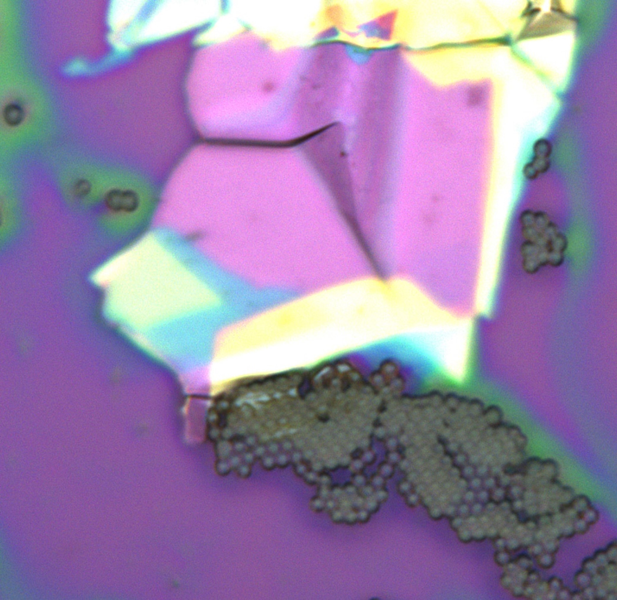
Single Photon Sources
Single-photon emission (SPE) is a quantum optical phenomenon where an emitter releases one photon at a time. This property is crucial for quantum technologies such as quantum cryptography, quantum computing, and photonic quantum networks. Our work focuses on developing SPE sources using two-dimensional (2D) materials. The 2D materials have introduced a new class of quantum emitters with unique advantages, including tunability, integrability, and strong light-matter interactions. Several families of 2D materials have the potential to have single-photon emission, including Transition Metal Dichalcogenides (TMDCs), Hexagonal Boron Nitride (hBN), Graphene Quantum Dots (GQDs) and Other 2D Allotropes. Currently, we are working on TMDC monolayers to make SPE sources from which single-photon emitters typically arise from localized excitons trapped in defect states or strain-induced potential wells.

Quantum Lasers
Quantum lasers based on 2D materials and their heterostructures integrated with nanocavities form a cutting-edge platform for developing compact, efficient, and tunable coherent light sources. These systems exploit the unique optical properties of intralayer and interlayer excitons in 2D materials, such as transition metal dichalcogenides (TMDs) and their type-II heterostructures. Intralayer excitons confined within individual 2D layers exhibit high radiative recombination rates and sharp emission spectra, while interlayer excitons formed across heterostructure interfaces provide longer lifetime and tunable emission energies due to their spatially separated electron-hole pairs. Integrating high-quality nanocavities further enhances light-matter interactions, facilitating strong coupling towards low-threshold lasing. By harnessing these excitonic properties, quantum lasers based on 2D materials and heterostructures offer promising applications in quantum information processing, photonics, and on-chip optical communications.
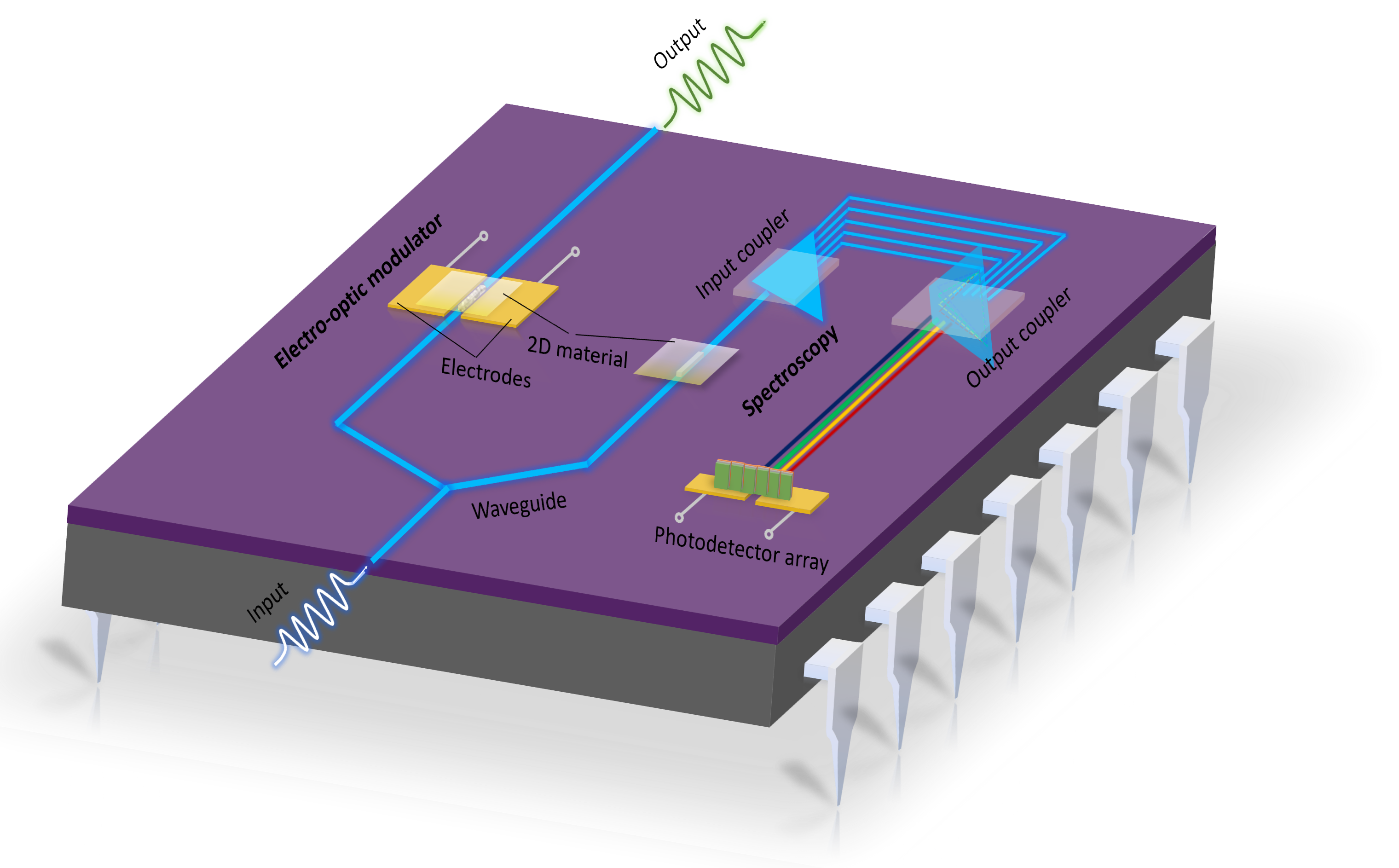
Photonic Devices and circuits for Lab-On-Chip
The development of advanced photonic devices towards Lab-on-a-chip technology is another research direction with two-dimensional materials. These materials offer a great viable platform for the development of ultra-compact, flexible, and multifunctional devices for wearable and Lab-on-a-chip technologies. Due to their angstrom scale thicknesses & flexibility, we can envision transparent electronic or photonic circuits. They can empower future technologies with wearable transparent- wristwatches, cardiac monitors & stimulators, stress monitors & controllers, and household windows for generating electricity through solar radiation. The Lab-on-a-chip technology integrates multiple devices onto a single miniaturized chip and synchronizes different functional operations finding applications in agricultural, biomedical, chemical, automobile, communications, spectroscopy, and photonics applications. The key component of the Lab-on-a-chip device is a light source (laser) which should be compatible with chip dimensions, and this is a quest of research for the development of such sources.
Non-linear Optics and Optoelectronics
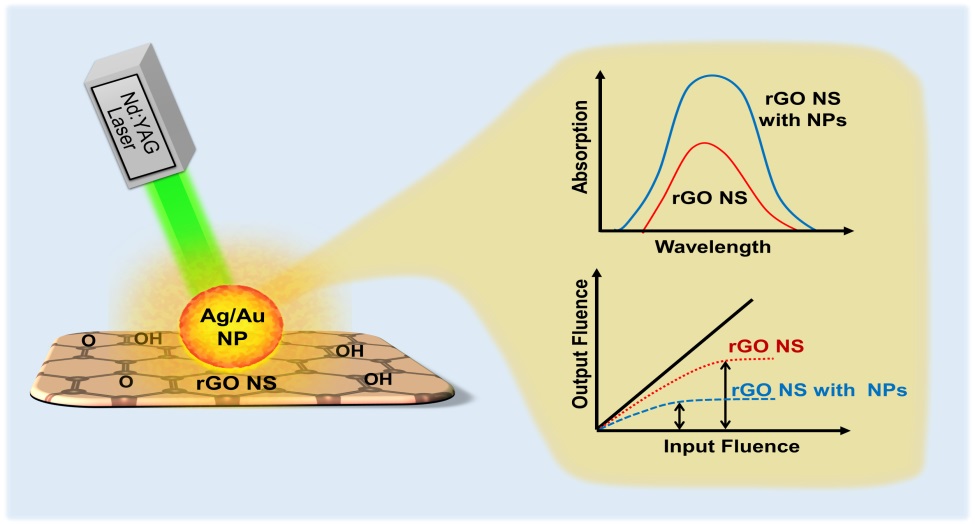
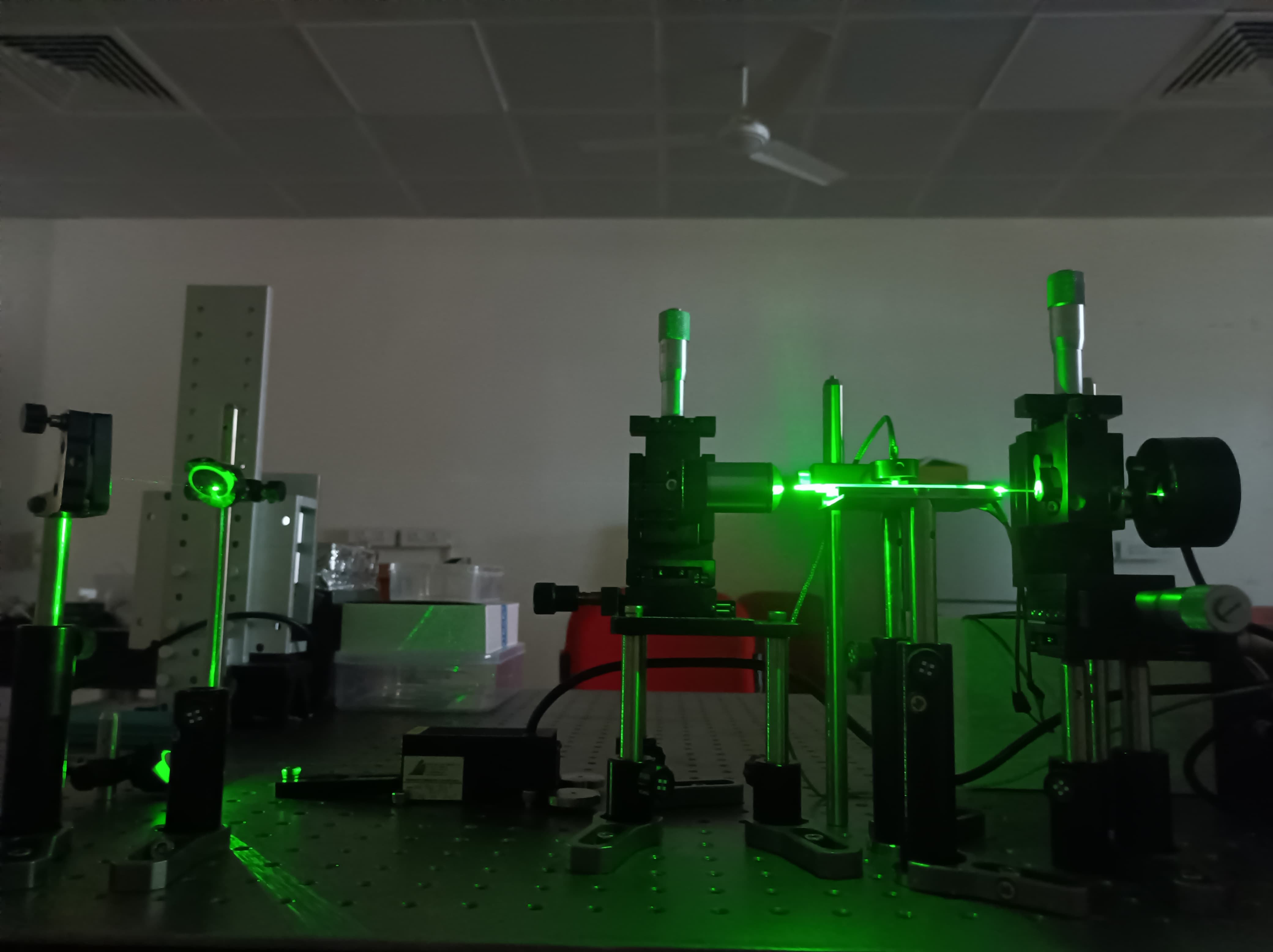
Our research interest is centered on the dynamic field of nonlinear optics and optoelectronic of vdW heterostructures and functionalized 2D materials. We majorly focus on the exploration of enhanced light-matter interactions in various 2D-based systems. In nonlinear optics, we aim to understand and harness the nonlinear optical absorption effects to address real-world challenges and drive technological innovation. We use the Z-scan experiment, an indispensable tool for probing the optical nonlinearities of various materials. Optoelectronic properties involve electrical characterizations of 2D-based systems to find efficient materials for light sensing, light-emitting, and solar cell applications. We plan to explore the integration of 2D materials with various kinds of functional units to expand the use of 2D material science in emerging fields of wearable electronics and flexible displays.
Optical Fiber Sensors
The development of Novel Optical Fiber Sensors based on Surface Plasmon Resonance (SPR) and Evanescent Wave (EW) Fields using thin sensing films for futuristic applications. By efficiently using the property of intensity modulation or wavelength shift in response of optical fiber induced by the change in refractive index of surroundings. The humidity or gas sensing and strain/pressure sensing have applications including structural health monitoring. Optical Fiber Sensors are better in sensing due to the capabilities including zero electromagnetic interference, remote sensing, and fast response mechanism. We aim to innovate and design cost-efficient, high sensitive, fast response, easy to fabricate, & robust optical fiber sensors.
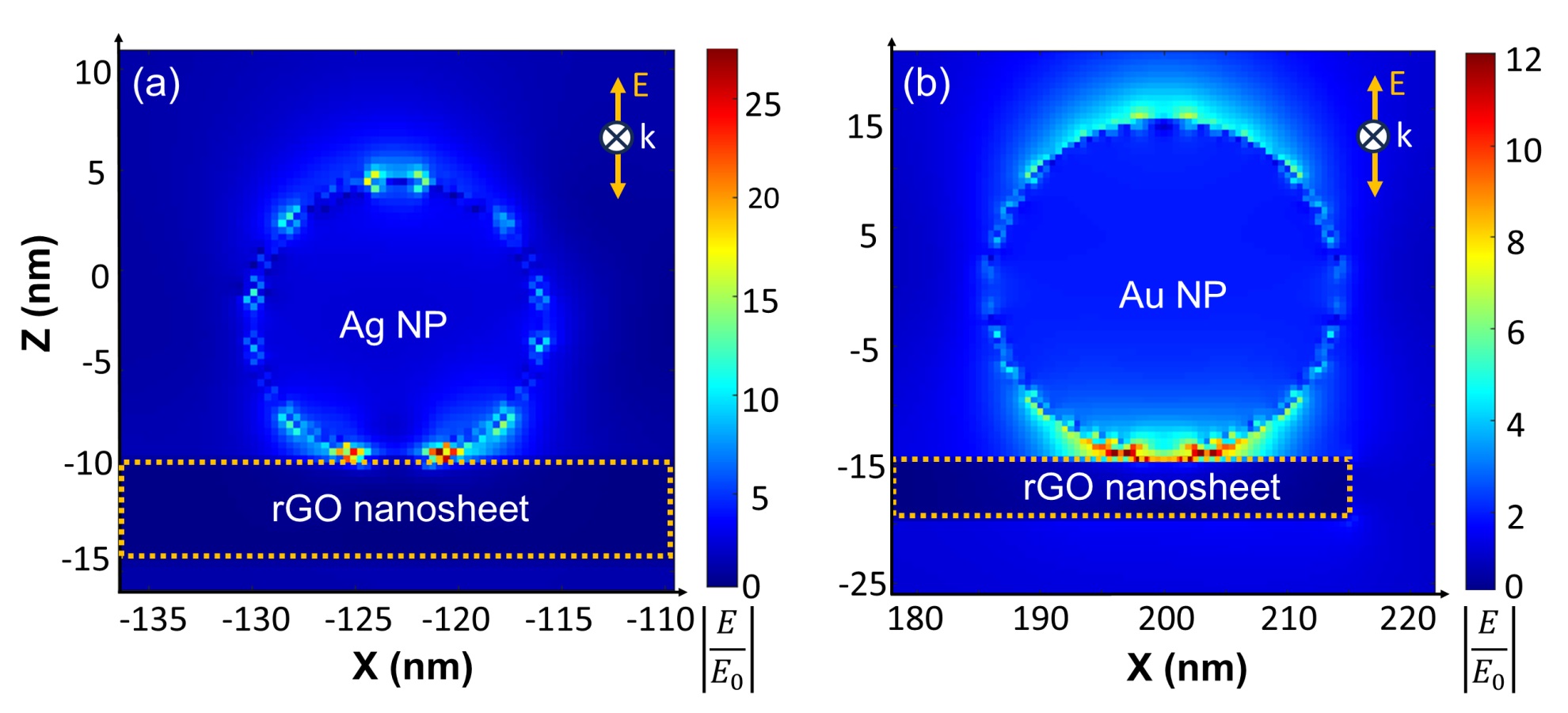
Theoretical & Computational Optical Physics
Optical physics through theoretical & computational frameworks helps to understand the light-matter interactions in 2D materials and doped/functionlized 2D materilas. Using the finite-difference time-domain (FDTD) method, we can simulate the complex interplay of electromagnetic fields with nanostructures and materials at the nanoscale. This approach enables precise modeling of phenomena such as enhanced light confinement, strong coupling effects, and plasmon-exciton interactions. By leveraging FDTD simulations, it is possible to optimize the design of photonic crystal cavities and plasmonic nanoparticle assemblies to maximize the optical response of 2D materials, paving the way for advanced applications in quantum optics, photonic circuits, and nanoscale light sources.